Introduction
AVR microcontroller was developed in 1996 by Atmel Company, and the architecture of the AVR micro controller was developed by Vegard Vollan and Alf Egil Bogen. The name of AVR is derived from its developers. AVR stands for Alf-Egil-Bogen-Vegard-Wollan-RISC Microcontroller and also known as Advanced Virtual RISC Microcontroller. The first microcontroller AT90S8515 was based on AVR architecture, but the first microcontroller to hit the business was AT90S1200 in the year 1997. The speed of the AVR microcontroller is high when compared to the PIC and 8051 microcontroller .
The AVR was one of the first microcontroller families to use on-chip flash memory for program storage, as opposed to OTP ROM, EPROM or EEPROM used by other microcontrollers at that time.ATmega & Xmega AVR chips became extremely popular after they were designed into the 8-bit Arduino platform.

Atmel , AVR microcontrollers (MCUs) are very easy to use. All AVR microcontrollers require Integrated Development Environment(IDE) such as Atmel Studio. Using this IDE, we can create, compile, and debug programs on all AVR microcontrollers.Atmel Studio is available free of charge. To download and install the latest Atmel studio use this link.
Family of AVR Microcontroller–

AVRs Microcontroller are generally classified into following:
- tinyAVR — the ATtiny series
- 0.5–16 kB program memory
- 6–32-pin package
- Limited peripheral set
- megaAVR — the ATmega series
- 4–512 kB program memory
- 28–100-pin package
- Extended instruction set (multiply instructions and instructions for handling larger program memories)
- Extensive peripheral set
- XMEGA — the ATxmega series
- 16–384 kB program memory
- 44–64–100-pin package (A4, A3, A1)
- Extended performance features, such as DMA, “Event System”, and cryptography support.
- Extensive peripheral set with ADCs
- Application-specific AVR
- megaAVRs with special features not found on the other members of the AVR family, such as LCD controller, USB controller, advanced PWM, CAN, etc.
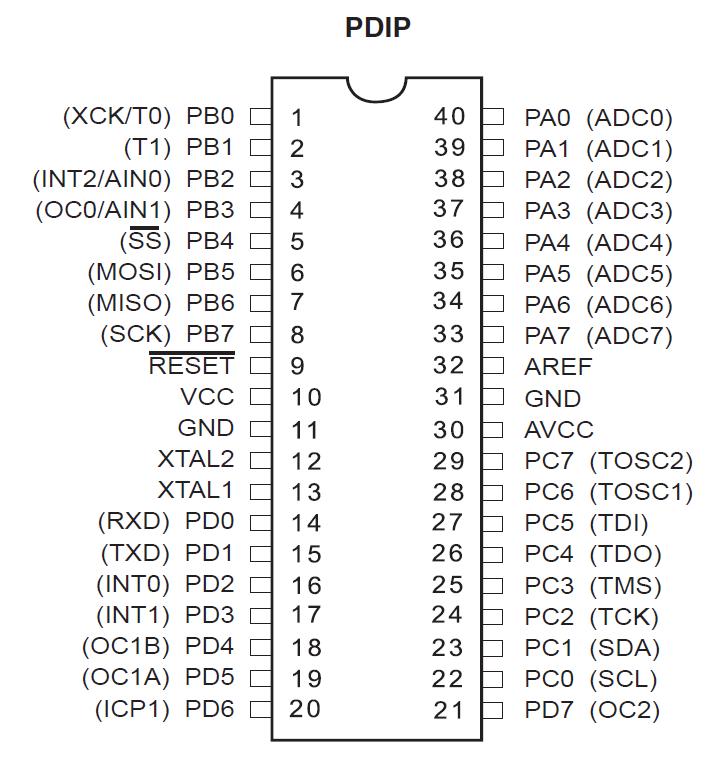
Atmega32 pin diagram
Pin Configurations PDIP package-
PIN count: Atmega32 has got 40 pins. Two for Power (pin no.10: +5v, pin no. 11: ground), two for oscillator (pin 12, 13), one for reset (pin 9), three for providing necessary power and reference voltage to its internal ADC, and 32 (4×8) I/O pins.


About I/O pins: ATmega32 is capable of handling analogue inputs. Port A can be used as either DIGITAL I/O Lines or each individual pin can be used as a single input channel to the internal ADC of ATmega32, plus a pair of pins AREF, AVCC & GND (refer to ATmega32 datasheet) together can make an ADC channel.
No pins can perform and serve for two purposes (for an example: Port A pins cannot work as a Digital I/O pin while the Internal ADC is activated) at the same time. It’s the programmers responsibility to resolve the conflict in the circuitry and the program.
Digital I/O pins: ATmega32 has 32 pins (4portsx8pins) configurable as Digital I/O pins.
Timers: 3 Inbuilt timer/counters, two 8 bit (timer0, timer2) and one 16 bit (timer1).
ADC: It has one successive approximation type ADC in which total 8 single channels are selectable. They can also be used as 7 (for TQFP packages) or 2 (for DIP packages) differential channels. Reference is selectable, either an external reference can be used or the internal 2.56V reference can be brought into action. There external reference can be connected to the AREF pin.
Communication Options: ATmega32 has three data transfer modules embedded in it. They are
- SPI
- USART
- Serial Peripheral Interface
- I2C
Pin Configurations TQFP/MLF package-


VCC-Digital supply voltage.
GND-Ground.
Port A (PA7..PA0)-Port A serves as the analog inputs to the A/D Converter.Port A also serves as an 8-bit bi-directional I/O port, if the A/D Converter is not used. Port pin scan provide internal pull-up resistors (selected for each bit). The Port A output buffers have symmetrical drive characteristics with both high sink and source capability. When pins PA0 to PA7are used as inputs and are externally pulled low, they will source current if the internal pull-up resistors are activated. The Port A pins are tri-stated when a reset condition becomes active,even if the clock is not running.
Port B (PB7..PB0)-Port B is an 8-bit bi-directional I/O port with internal pull-up resistors (selected for each bit). The Port B output buffers have symmetrical drive characteristics with both high sink and source capability. As inputs, Port B pins that are externally pulled low will source current if the pull-up resistors are activated. The Port B pins are tri-stated when a reset condition becomes active,even if the clock is not running.
Port C (PC7..PC0)-Port C is an 8-bit bi-directional I/O port with internal pull-up resistors (selected for each bit). The Port C output buffers have symmetrical drive characteristics with both high sink and source capability. As inputs, Port C pins that are externally pulled low will source current if the pull-up resistors are activated. The Port C pins are tri-stated when a reset condition becomes active,even if the clock is not running. If the JTAG interface is enabled, the pull-up resistors on pinsPC5(TDI), PC3(TMS) and PC2(TCK) will be activated even if a reset occurs.The TD0 pin is tri-stated unless TAP states that shift out data are entered.
Port D (PD7..PD0)-Port D is an 8-bit bi-directional I/O port with internal pull-up resistors (selected for each bit). The Port D output buffers have symmetrical drive characteristics with both high sink and source capability. As inputs, Port D pins that are externally pulled low will source current if the pull-up resistors are activated. The Port D pins are tri-stated when a reset condition becomes active,even if the clock is not running.
RESET-Reset Input. A low level on this pin for longer than the minimum pulse length will generate a reset, even if the clock is not running. Shorter pulses are not guaranteed to generate a reset.
XTAL1-Input to the inverting Oscillator amplifier and input to the internal clock operating circuit.
XTAL2-Output from the inverting Oscillator amplifier.
AVCC-AVCC is the supply voltage pin for Port A and the A/D Converter. It should be externally connected to VCC, even if the ADC is not used. If the ADC is used, it should be connected to VCCthrough a low-pass filter. AREF-AREF is the analog reference pin for the A/D Converter.
Analog comparator: On-chip analog comparator is available. An interrupt is assigned for different comparison result obtained from the inputs.
External Interrupt: 3External interrupt is accepted. Interrupt sense is configurable.
Memory: It has 32Kbytes of In-System Self-programmable Flash program memory, 1024 Bytes EEPROM, 2Kbytes Internal SRAM. Write/Erase Cycles: 10,000 Flash / 100,000 EEPROM.
Clock: It can run at a frequency from 1 to 16 MHz. Frequency can be obtained from external Quartz Crystal, Ceramic crystal or an R-C network. Internal calibrated RC oscillator can also be used.
More Features: Up to 16 MIPS throughput at 16MHz. Most of the instruction executes in a single cycle. Two cycle on-chip multiplication. 32 × 8 General Purpose Working Registers
Debug: JTAG boundary scan facilitates on chip debug.
Operating Voltages– 2.7V – 5.5V for ATmega32L and 4.5V – 5.5V for ATmega32.
Power Consumption at 1MHz, 3V, 25°C– Active: 1.1mA– Idle Mode: 0.35mA– Power-down Mode: < 1μA
Programming: Atmega32 can be programmed either by In-System Programming via Serial peripheral interface or by Parallel programming. Programming via JTAG interface is also possible. Programmer must ensure that SPI programming and JTAG are not be disabled using fuse bits; if the programming is supposed to be done using SPI or JTAG.
Atmega32 block diagram–


Leave a comment