
Introduction of 8051
The 8051 is a Harvard architecture, CISC instruction set, single chip microcontroller (µC) series which was developed by Intel in 1980 for use in embedded systems. Intel’s original MCS-51 family was developed using NMOS technology, but later it is modified with CMOS technology and referred as 80C51which consume less power than their NMOS predecessors and gives high switching speed than NMOS technology. This made them more suitable for battery-powered devices. Nowadays there are many variants of 8051 core which is capable of processing 8/16/32-bit at a time, Earlier family is limited to 8-bit processing only. While Intel no longer manufactures 8051 cored controller or its derivatives, enhanced binary compatible derivatives made by numerous vendors remain popular today like Atmel’s AT89C51 and its derivatives, NXP’s P89v51 and its derivatives, etc. Some derivatives integrate a digital signal processor (DSP). In addition to these physical devices, several companies also offer MCS-51 derivatives as IP cores for use in FPGAs or ASICs designs.
As years passed by, the quality of technology surpassed the expectation of the greatest minds, with gadgets becoming smaller, sleeker and more efficient. Microcontrollers were seen as the answer to the requirements raised in advanced electronics. This is the reason why manufacturers have now focused their production around the following main developmental aspects:
- Ease-of-use
- Market availability
- Less power usage
- Smaller processing power
- More integrated features like RF and USB
- Smaller form factors
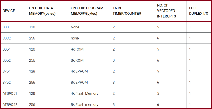
Some of the 8051’s derivatives are given as follows:
Microcontroller 8051 is basic among all the MCUs and excellence for beginners.Here we use AT89C51, in which AT mean ATMEL, C mean CMOS technology. and rest numbers indicates family identification.
8051 is an 8-bit microcontroller which means that most available operations are limited to 8 bits.
Features of 8051 microcontroller
- 4 KB on chip program memory.
- 128 bytes on chip data memory(RAM).
- 128 user defined software flags.
- 8-bit data bus
- 16-bit address bus
- 32 general purpose registers each of 8 bits
- 16 bit timers (usually 2, but may have more, or less).
- 3 internal and 2 external interrupts.
- Bit as well as byte addressable RAM area of 16 bytes.
- Four 8-bit ports, (short models have two 8-bit ports).
- 16-bit program counter and data pointer.
- 1 Microsecond instruction cycle with 12 MHz Crystal.
- Harvard Memory Architecture – It has 16 bit Address bus (each of RAM and ROM) and 8 bit Data Bus.
- 8051 can execute 1 million one-cycle instructions per second with a clock frequency of 12MHz.
- This microcontroller is also called as “System on a chip” because it has all the features on a single chip.
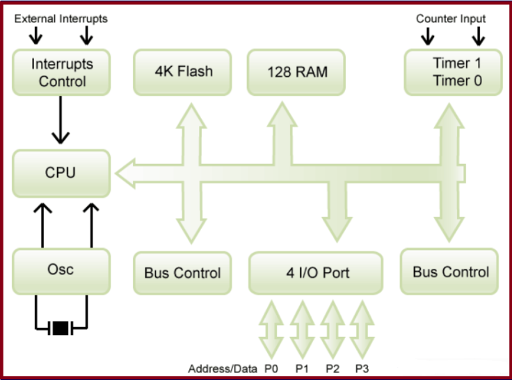
The Block Diagram of 8051 Microcontroller
Description of AT89C51
- The AT89C51 is a low-power, high-performance CMOS 8-bit microcomputer with 4 Kbytes of Flash Programmable and Erasable Read Only Memory (EEPROM). The device is manufactured using Atmel’s high density nonvolatile memory technology and is compatible with the industry standard MCS-51 instruction set and pin-out.
- The on-chip Flash allows the program memory to be reprogrammed in-system or by a conventional nonvolatile memory programmer. By combining a versatile 8-bit CPU with Flash on a monolithic chip, the Atmel AT89C51 is a powerful microcomputer which provides a highly flexible and cost effective solution to many embedded control applications.
- The AT89C51 provides the following standard features: 4Kbytes of Flash, 128 bytes of RAM, 32 I/O lines, two 16-bit timer/counters, a five vector two-level interrupt architecture, a full duplex serial port, on-chip oscillator and clock circuitry. In addition, the AT89C51 is designed with static memory.
- Logic for operation down to zero frequency and supports two software selectable power saving modes.
Pinout of AT89C51
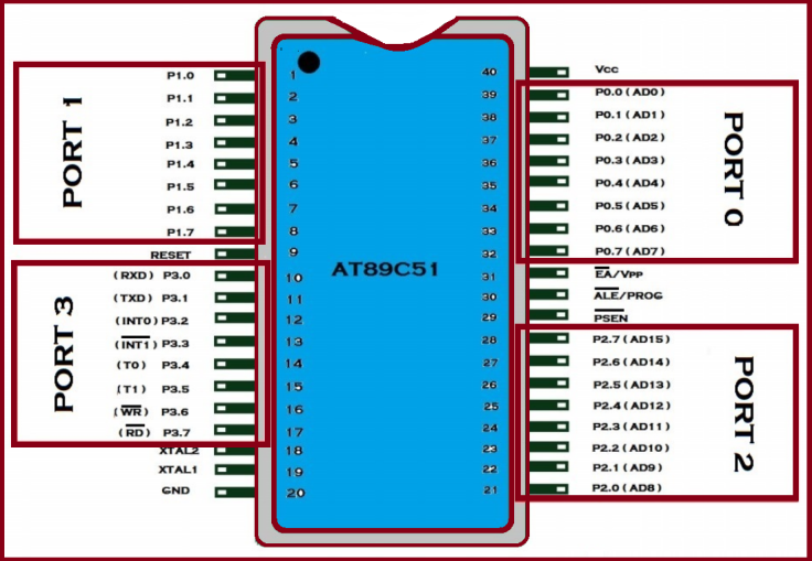
Pins 1-8: Port 1 Each of these pins can be configured as an input or an output.
Pin 9: RESET A logic one on this pin disables the microcontroller and clears the contents of most registers. In other words, the positive voltage on this pin resets the microcontroller. By applying logic zero to this pin, the program starts execution from the beginning.
Pin 10: RXD Serial asynchronous communication input or Serial synchronous communication output.
Pin 11: TXD Serial asynchronous communication output or Serial synchronous communication clock output.
Pin 12: INT0 Interrupt 0 input.
Pin 13: INT1 Interrupt 1 input.
Pin 14: T0 Counter 0 clock input.
Pin 15: T1 Counter 1 clock input.
Pin 16: WR Write to external (additional) RAM.
Pin 17: RD Read from external RAM.
Pin 18, 19: X2, X1 Internal oscillator input and output. A quartz crystal which specifies operating frequency is usually connected to these pins. Instead of it, miniature ceramics resonators can also be used for frequency stability. Later versions of microcontrollers operate at a frequency of 0 Hz up to over 50 Hz.
Pin 20: GND Ground.
Pin 21-28: Port 2 If there is no intention to use external memory then these port pins are configured as general inputs/outputs. In case external memory is used, the higher address byte, i.e. addresses A8-A15 will appear on this port. Even though memory with capacity of 64Kb is not used, which means that not all eight port bits are used for its addressing, the rest of them are not available as inputs/outputs.
Pin 29: PSEN If external ROM is used for storing program then a logic zero (0) appears on it every time the microcontroller reads a byte from memory.
Pin 30: ALE Prior to reading from external memory, the microcontroller puts the lower address byte (A0-A7) on P0 and activates the ALE output. After receiving signal from the ALE pin, the external register (usually 74HCT373 or 74HCT375 add-on chip) memorizes the state of P0 and uses it as a memory chip address. Immediately after that, the ALU pin is returned its previous logic state and P0 is now used as a Data Bus. As seen, port data multiplexing is performed by means of only one additional (and cheap) integrated circuit. In other words, this port is used for both data and address transmission.
Pin 31: EA By applying logic zero to this pin, P2 and P3 are used for data and address transmission with no regard to whether there is internal memory or not. It means that even there is a program written to the microcontroller, it will not be executed. Instead, the program written to external ROM will be executed. By applying logic one to the EA pin, the microcontroller will use both memories, first internal then external (if exists).
Pin 32-39: Port 0 Similar to P2, if external memory is not used, these pins can be used as general inputs/outputs. Otherwise, P0 is configured as address output (A0-A7) when the ALE pin is driven high (1) or as data output (Data Bus) when the ALE pin is driven low (0).
Pin 40: VCC +5V power supply.
Application
- Energy Management:Efficient metering systems help in controlling energy usage in homes and industrial applications. These metering systems are made capable by incorporating microcontrollers.
- Touch screens:A high number of microcontroller providers incorporate touch-sensing capabilities in their designs. Portable electronics such as cell phones, media players and gaming devices are examples of microcontroller-based touch screens.
- Automobiles: The 8051 finds wide acceptance in providing automobile solutions. They are widely used in hybrid vehicles to manage engine variants. Additionally, functions such as cruise control and anti-brake system have been made more efficient with the use of microcontrollers.
- Medical Devices:Portable medical devices such as blood pressure and glucose monitors use microcontrollers will to display data, thus providing higher reliability in providing medical results.

Leave a comment